
Spending Energy to Gain Energy: A New CMOS Charger Architecture for Microsystems
18175_Inductively Coupled 180-nm CMOS Charger With Adjustable Energy-Investment Capability.
This paper presents a 180-nm CMOS inductively coupled charger that utilizes a programmable "Energy-Investment" technique to boost power extraction from miniaturized coils. By injecting battery energy into the pickup coil to increase in-phase current, the system achieves a significant output power increase, reaching up to 390 μW and demonstrating a 132% power boost at low coupling factors.
TL;DR
Researchers have developed a 180-nm CMOS charger that solves the "weak coupling" problem of tiny wireless sensors by proactively investing battery energy into the receiver coil. This technique, labeled Energy Investment, increases the coil's ability to "damp" the magnetic source, boosting harvested power by up to 132%—a critical breakthrough for devices where traditional resonant harvesting falls short.
Background: The "Small Coil" Bottleneck
In the world of IoT and biomedical implants, size is everything. However, as the pickup coil () shrinks, the coupling factor () between the transmitter and receiver drops drastically. This results in a millivolt-level induced EMF that is often too weak to overcome the system's own rectification thresholds or charging requirements.
Traditional SOTA systems rely on resonance to recycle energy. While effective, these systems are "frozen" into a specific optimal point; if the distance or orientation of the coil changes, the efficiency collapses.
The Core Insight: Inductive Energy Investment
The authors propose a counter-intuitive but mathematically sound strategy: Investment.
Instead of waiting for the induced EMF to slowly build up current in the coil, the system uses the onboard battery () to "kickstart" the current () in the coil. Because the energy stored in an inductor is quadratic (), the interaction between the large invested current and the small induced EMF creates a linear gain () that far exceeds what the EMF could produce on its own.
Methodology & Architecture
The system employs a bridge-like switch configuration () controlled by a synchronizer. The process follows four distinct phases:
- Energy Investment: Battery energy is pushed into the coil to reach a target .
- Energizing: The induced EMF contributes further energy to the coil.
- De-energizing: The combined energy (invested + harvested) is dumped back into the battery.
- Negative Cycle: The process repeats with reversed polarities to match the AC nature of induction.
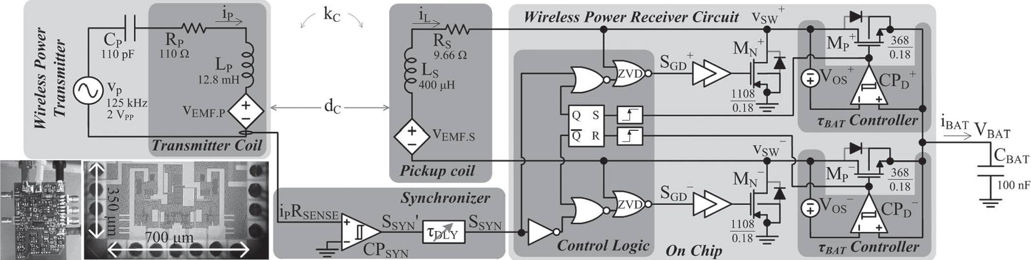 Figure 1: The investment-assisted CMOS IC architecture showing the control logic and the power stage.
Balancing the Scales: The Optimal Investment Point
You can't invest infinitely. The paper identifies two critical limits that define the "Max Power Point":
- Conduction Losses (): Resistive losses grow quadratically with the investment current (). Eventually, the cost of investing outweighs the harvested gain.
- Overdamping: If too much power is drawn, it actually reduces the current in the transmitter coil (), causing the source voltage to collapse.
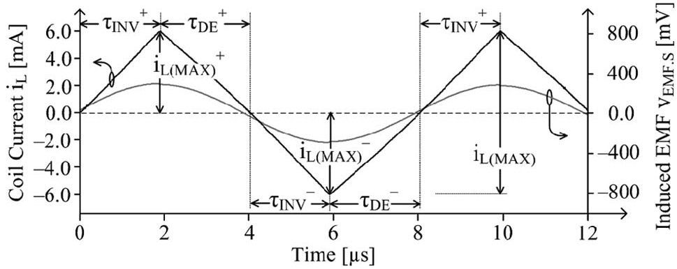 Figure 2: Measured results showing how battery power () peaks at an optimal investment level before conduction losses dominate.
Experimental Results
Prototyped in a 180-nm CMOS process, the chip was tested across various coupling scenarios:
- Low Coupling (): Output power jumped from a baseline to 82 μW, a 132% increase.
- High Coupling (): Output power reached 392 μW, a 24% increase.
The ability to adjust the investment level (controlled via comparator offsets ) allows this chip to adapt to different distances ()—a functionality that fixed-resonant and passive rectifiers lack.
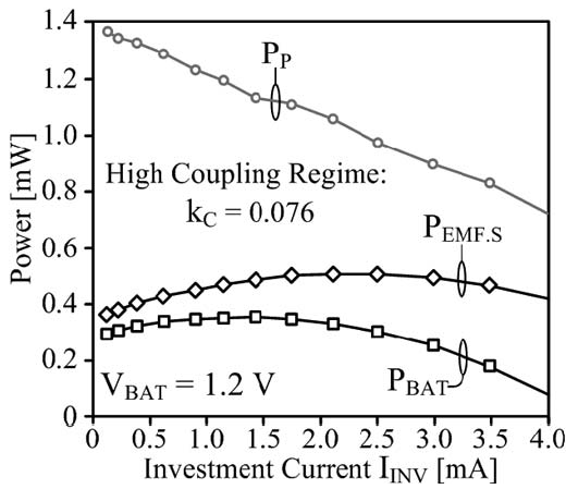 Figure 3: Maximum output power vs. coupling factor, illustrating the broad applicability of the programmable investment strategy.
Critical Insight & Future Outlook
This work highlights that for micro-scale energy harvesting, efficiency is not the only metric—net power is. By sacrificing some battery energy to increase the damping of the source, we can pull significantly more total energy into the system.
Future Work: The next step for this technology is the integration of an autonomous "Maximum Power Point Tracking" (MPPT) logic that can dynamically sense the coupling factor and adjust the investment time () in real-time, eliminating the need for manual tuning and making wireless sensors truly "set and forget."
Conclusion
The "Investment-Assisted Charger" marks a transition from reactive to proactive power management in wireless systems. It proves that even with the tiniest coils and weakest fields, we can still achieve high-performance charging by intelligently leveraging the energy we already have.