
3-D Printing: The "Poor Man's Cleanroom" for MEMS Education
11294_3-D Printing as an Effective Educational Tool for MEMS Design and Fabrication.
This paper introduces a cost-effective educational framework for MEMS (Microelectromechanical Systems) design using 3-D printing as a proxy for expensive cleanroom fabrication. By scaling up micro-scale architectures into macro-scale 3-D printed models, the method enables students to visualize and validate complex multilayer fabrication processes and crystalline orientations without high-vacuum equipment.
TL;DR
Microelectromechanical Systems (MEMS) are notoriously difficult to teach without a multi-million dollar cleanroom. This paper presents a breakthrough pedagogical shift: using 3-D printing to emulate micro-fabrication. By scaling microscopic devices (switches, inductors) into macroscopic 3-D printed models, students learn the "Why" and "How" of Miller indices, etching, and sacrificial layers through physical interaction rather than dry theory.
The Problem: The High Wall of Cleanroom Education
Teaching MEMS is a logistical nightmare for most universities. To truly understand how a capacitive switch works, a student ideally needs to fabricate one. However:
- Cleanrooms are expensive: High-vacuum equipment and chemical safety protocols are beyond the budget of many undergraduate programs.
- The Abstraction Gap: Concepts like Miller indices ([100] vs [110] planes) and anisotropic etching are highly mathematical. Without physical models, students resort to memorizing diagrams rather than developing an intuitive "feel" for material science.
Methodology: Scaling the Micro to the Macro
The authors propose a "Pseudo-Fabrication" workflow. The core insight is that the constraints of 3-D printing (resolution, layer adhesion, support material) remarkably mirror the constraints of lithography and etching.
1. Visualizing the Lattice (Assignment 1)
Students calculate angles for crystalline planes and use CAD software to "extract" these planes from a virtual silicon wafer. Printing these helps them touch the difference between a [100] and [110] oriented wafer.
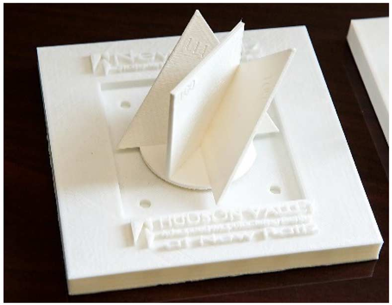 Fig 1: From mathematical illustration to a 3-D printed crystalline lattice.
2. The Geometry of Etching (Assignment 2)
Instead of just drawing an "anisotropic etch," students must model the undercut and over-etch in SolidWorks based on etchant depth and mask geometry. This forces them to use trigonometry to predict physical shapes.
3. The Full Workflow: MEMS Capacitive Switch
The "Capstone" of the course involves building a functional-looking MEMS switch.
- The Sacrificial Layer: In real MEMS, a sacrificial layer is etched away to "release" a moving part.
- The 3-D Analog: Students use the 3-D printer's support material as the sacrificial layer. By dissolving the support in a water-based bath (SCA-1200 system), they replicate the "Release Etch" process used in cleanrooms.
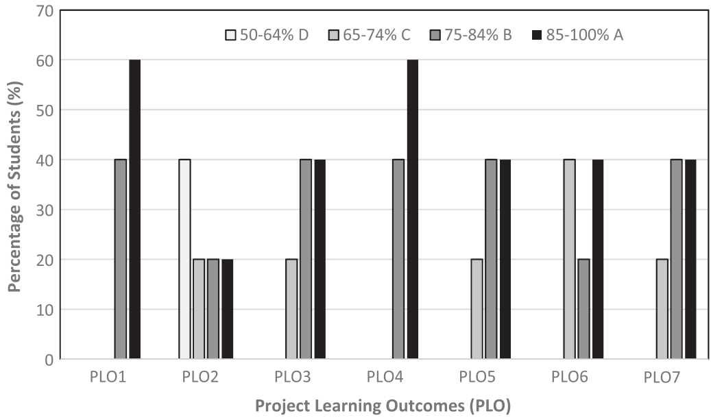 Fig 2: Layer-by-layer breakdown of a MEMS inductor, emulating the mask-and-deposit workflow of real semiconductor manufacturing.
Experiments & Results: Does It Actually Work?
The authors compared exam scores from Fall 2013 (Traditional) to Fall 2014 (3-D Printing Integrated).
- Evidence of Success: Performance on the "Fabrication Design" question on the final exam (Q3) saw a massive boost. This indicates that physically modeling the layers helped students internalize the step-by-step logic of manufacturing.
- Student Sentiment: Surveys showed overwhelming "Strong Agreement" that the modules engaged their interest.
- The "SolidWorks" Hurdle: Interestingly, 40% of students struggled with the CAD modeling (PLO2). This highlights a critical insight: the bottleneck in modern engineering education isn't just the hardware (the printer), but the digital fluency (CAD skills) required to pilot it.
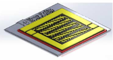 Fig 3: Quantifiable improvement in student performance across three key Learning Outcomes (CLOs).
Critical Insight & Future Outlook
This paper proves that fidelity of concept is more important than fidelity of scale. A student does not need to handle a 10-micron beam to understand "residual stress" or "conformal coating." By scaling the device up 35x, the physics remains relatable, and the errors become visible to the naked eye.
Limitations: The 3-D printer used (Dimension 1200es) has a resolution limit (254µm), which prevents the creation of truly intricate MEMS features.
Future Work: The authors suggest moving into SLA (Stereolithography) printing for higher resolution and adding "actuation" (movement) to the models to teach the mechanics of MEMS, not just the static geometry. This approach is a blueprint for any institution looking to democratize high-tech engineering education on a budget.