
All-NMOS Three-Level SC Converter: Redefining Power Density for Industrial Sensors
13178_Design of Monolithic All-NMOS Three-Level Three-phase Switched-Capacitor Power Converter for Industrial Environmental Sensor Conditioning.
Summary
Problem
Method
Results
Takeaways
Abstract
This paper introduces a monolithic, all-NMOS three-level switched-capacitor (SC) power converter designed for industrial sensor conditioning. It features a unique tri-mode operation and a three-phase interleaving scheme, achieving a high conversion ratio (CR > 4:1) and a power density of 125 mW/mm² on a 0.35-µm BCD process.
## Executive Summary
**TL;DR**: This paper presents a breakthrough in monolithic power management by introducing a three-level Switched-Capacitor (SC) converter that achieves a high conversion ratio (>4:1) from a 6V input using only thin-oxide devices. By moving beyond traditional dual-mode operation to a **tri-mode operation**, the design significantly reduces voltage stress, enabling high power density (125 mW/mm²) and improved efficiency in a standard 0.35-µm BCD process.
**Background**: In the landscape of industrial IoT, sensors often require isolated power supplies where rectifiers output 5-6V, while core electronics operate at ~1.2V. Shrinking these converters onto a single chip while maintaining high input tolerance is a classic "Power Density vs. Reliability" trade-off.
## The Innovation Gap: Why Multi-Level?
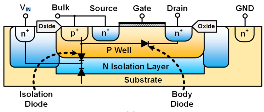
The primary bottleneck in integrated SC converters is the **Breakdown Voltage (BV)**. Using high-BV devices requires thicker gate oxides and lighter doping, which results in higher ON-resistance ($R_{ON}$) and lower capacitance density. This kills efficiency and inflates silicon area.
Conventional 4:1 topologies like Dickson or Serial-Parallel have a "weakest link" problem—certain switches or capacitors are subjected to nearly the full input voltage. The authors' insight was to adapt the **three-level switching** concept (common in inductive converters) to a capacitive architecture, creating a "safe haven" intermediate voltage rail.
## Methodology: Tri-Mode Operation and All-NMOS Power Stage
The core of this work is the transition from two phases to three distinct modes: **Charge, Hold, and Discharge**.
### 1. The Architecture
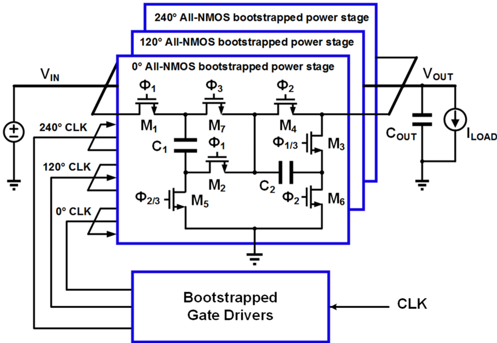
As shown in the architecture diagram, the converter uses two flying capacitors ($C_1, C_2$) and seven NMOS switches.
### 2. Physical Intuition of Tri-Mode
- **Phase 1 (Charge)**: $C_1$ and $C_2$ are in series, charged by $V_{IN}$.
- **Phase 2 (Hold)**: $C_1$ holds its charge while $C_2$ provides current to the output.
- **Phase 3 (Discharge)**: $C_1$ and $C_2$ are reconfigured so $C_1$ discharges into $C_2$ and the output.
This sequence ensures that the voltage across any single switch never exceeds $V_{IN}/2$, effectively doubling the voltage handling capability of the underlying process.
### 3. Three-Phase Interleaving
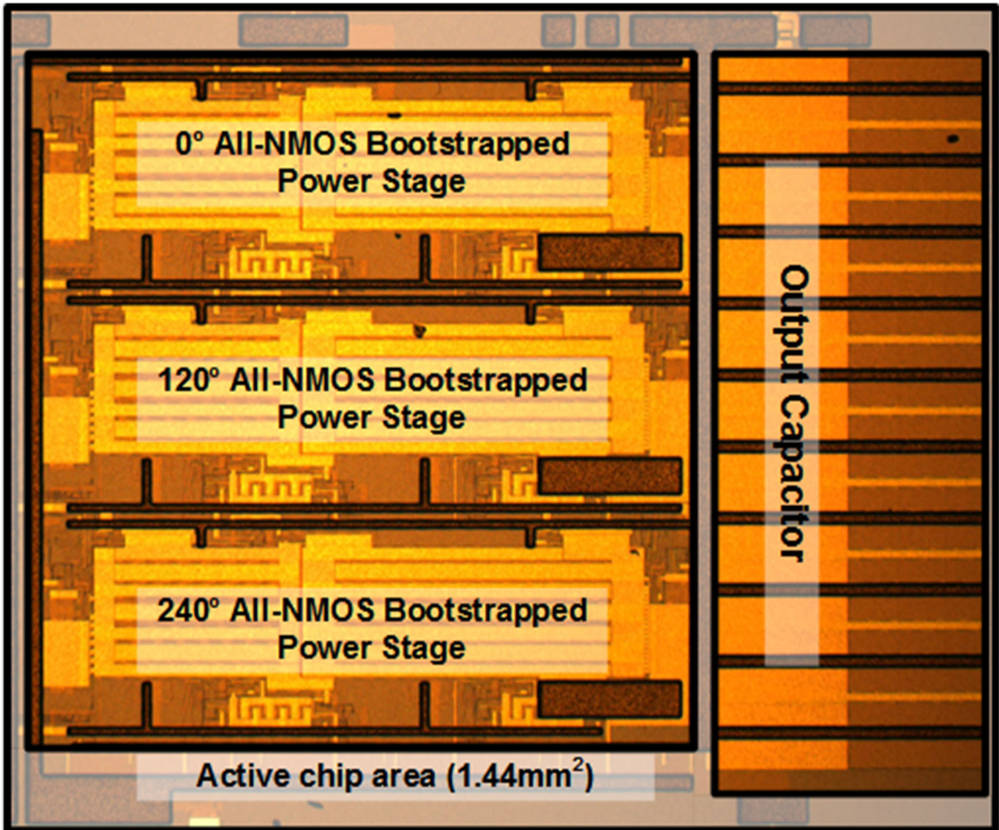
Because the charge delivery to the output is unbalanced across the three modes, the authors implemented a **three-phase interleaving scheme**. By shifting three power stages by 120°, the total output charge remains constant across all phases, drastically reducing the output ripple and the size of the required on-chip output capacitor.
## Performance and SOTA Comparison
The performance metrics validate the effectiveness of the tri-mode approach. With a 6V input, the converter achieves:
- **Power Density**: 125 mW/mm², which is remarkably high for a 4:1 conversion ratio on a 0.35-µm process.
- **Efficiency**: Peak efficiency of 64.3%. While some low-voltage converters reach 80%+, this design's value lies in its ability to handle high input voltages without external components.
- **Equivalent Resistance ($R_{OUT}$)**: The authors mathematically prove that their topology results in an 18% lower output resistance compared to classic Dickson or Serial-Parallel converters, which directly translates to higher power delivery capability.
## Deep Insight & Conclusion
The "All-NMOS" design choice is critical—NMOS devices have 3-4x lower $R_{ON}$ per unit area than PMOS. By combining an all-NMOS stage with bootstrapped drivers and a multi-level topology, the authors have bypassed the traditional limits of the 0.35-µm BCD process.
**Takeaway**: This work proves that we don't always need advanced (and expensive) sub-100nm processes to achieve high power density. Intelligent topological innovation—specifically creating intermediate voltage rails internally—can extend the life and utility of mature semiconductor processes for high-voltage industrial applications.
**Limitations**: The peak efficiency (64.3%) is moderate. Future work could likely improve this by optimizing the bootstrap driver losses and exploring parasitic bottom-plate capacitance reduction.